01 / 02
ENJP

Top/Technology/3D-Stacked DRAM

3D-Stacked
DRAM

01 — How it works

Stack Memory
and Logic

Stacked Memory Wafers

Stack memory wafers vertically

Plane-wide Interconnect

Connect compute units and memory across the entire surface, minimizing interconnect length and maximizing connection density.

Logic Wafer

Perform efficient matrix operations based on the MN-Core architecture.

02 — Thermal design
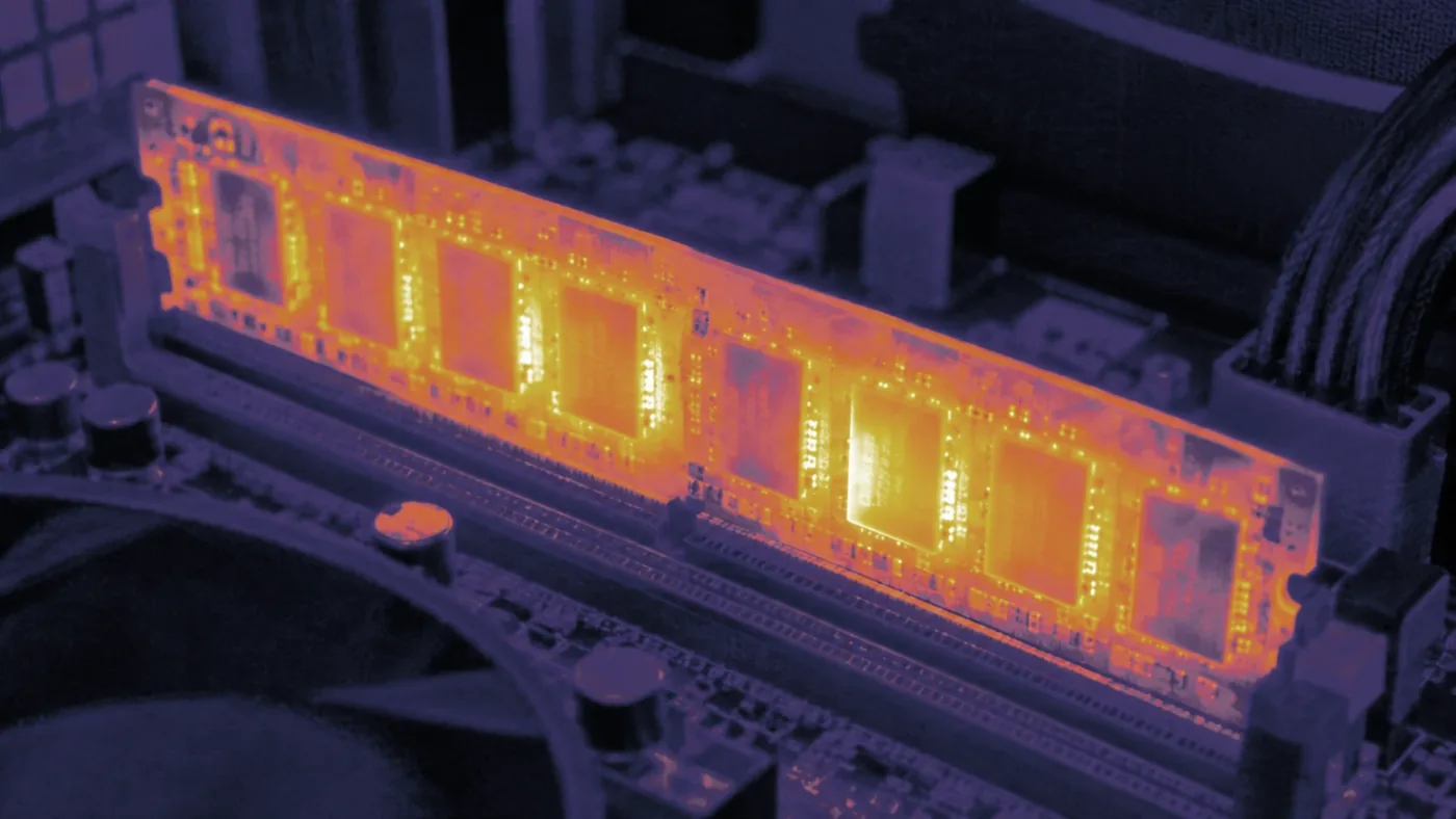
Thermal problem

Thermal image of a memory module in operation. The memory chips show the highest temperatures.

One of the major challenges in 3D-Stacked DRAM is thermal design. While AI chips generate substantial heat, memory is highly temperature-sensitive.

The MN-Core architecture delivers high power efficiency, which is precisely what makes 3D stacking possible.

See our power efficiency track record